
这个行业通常查什么
- Visual defects
- 2D dimensions
- Plating thickness
- Solder-joint cross-section
- Thermal reliability
客户最常问的一个问题
微米级焊点截面怎么制样才能不产生倒角与拖尾?
把试样尺寸、材料牌号与执行标准发给我们,工程师会给出判定方法与设备配置,可先寄样试测。
提交这个问题 →Packaging, PCB and precision structures need non-contact, high-magnification, automated judgment.
把试样尺寸、材料牌号与执行标准发给我们,工程师会给出判定方法与设备配置,可先寄样试测。
提交这个问题 →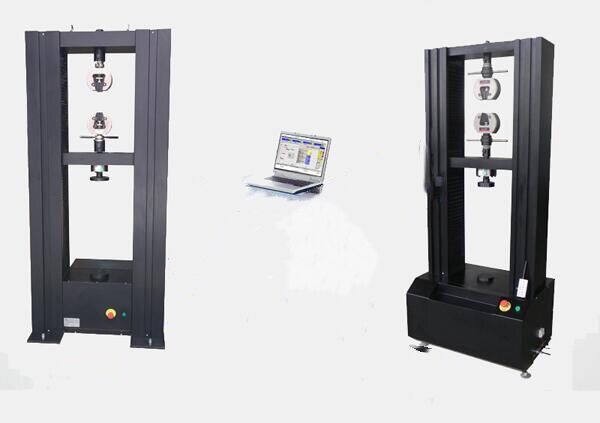
Electronic Universal Testing Machine
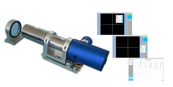
Photoelectric Autocollimator
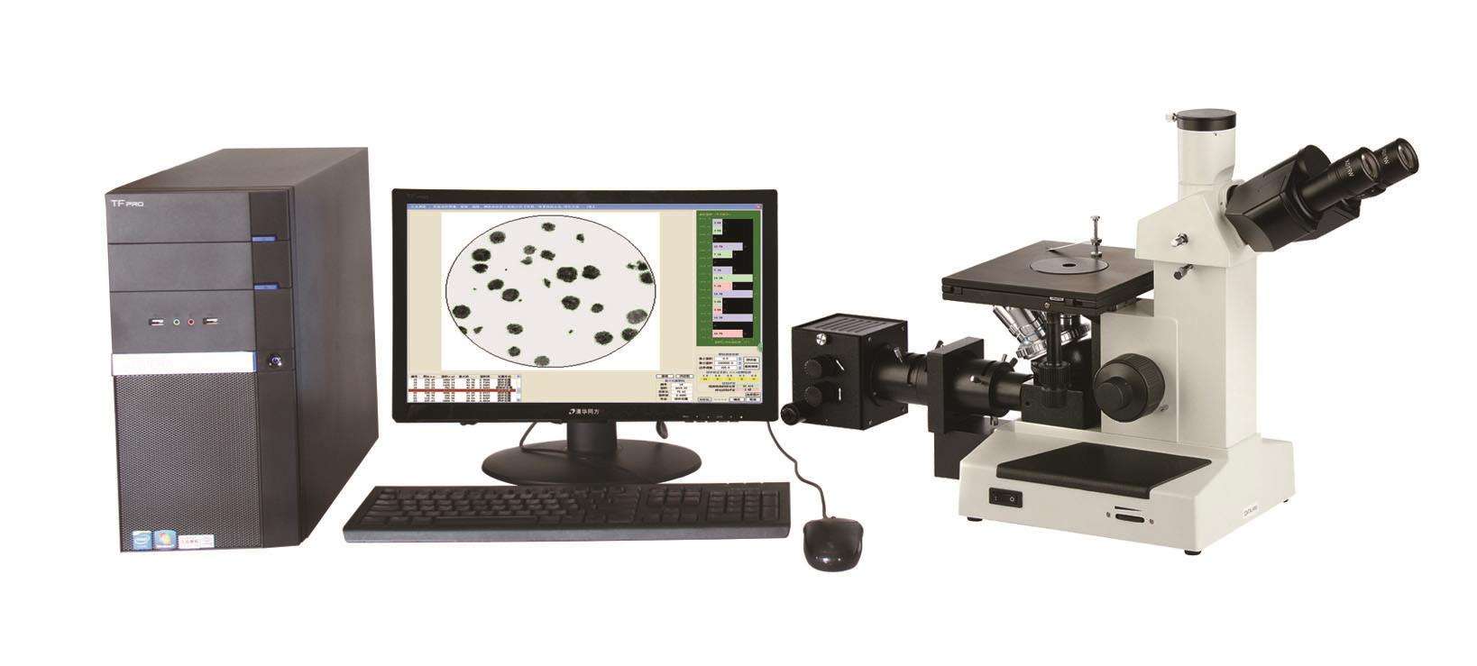
Metallurgical Microscope
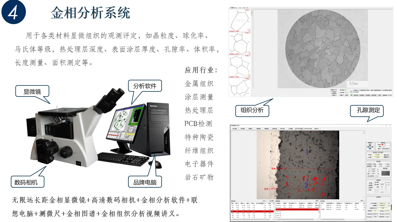
Metallurgical Microscope
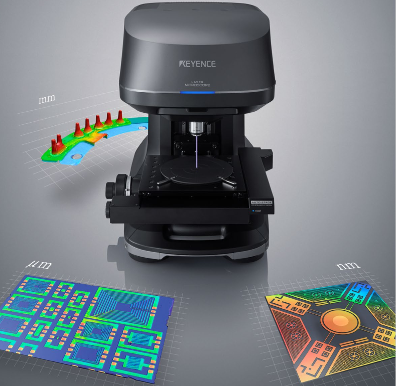
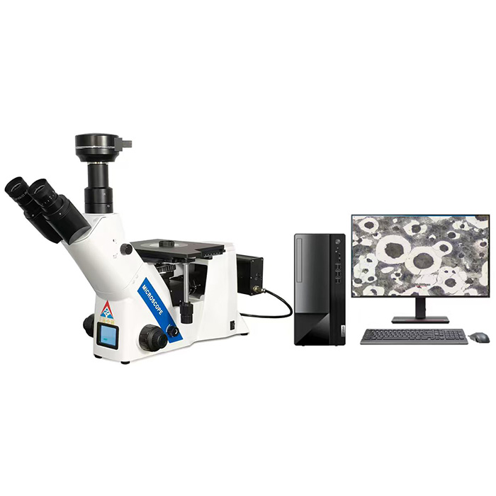
以上机型按行业常用配置排序;试样尺寸特殊或需要非标工装时,可按下单要求定制。
Lines are staffed 08:30–17:30 on business days. Leave a message after hours and we reply the next working day.
Call Us021-51693591 Email for a quotezhongyanyiqi@163.com Send a messageInclude material and specimen size for a faster answerShortlisted from our own range only; final specifications confirmed by our engineers. Full selection →